| This article includes a list of general references, but it lacks sufficient corresponding inline citations. Please help to improve this article by introducing more precise citations. (September 2017) (Learn how and when to remove this message) |
 POWER2 MCM POWER2 MCM | |
| General information | |
|---|---|
| Launched | 1993 |
| Designed by | IBM |
| Architecture and classification | |
| Instruction set | POWER ISA |
| History | |
| Predecessor | POWER1 |
| Successor | POWER3 |
| POWER, PowerPC, and Power ISA architectures |
|---|
| NXP (formerly Freescale and Motorola) |
| IBM |
|
| IBM/Nintendo |
| Other |
| Related links |
| Cancelled in gray, historic in italic |
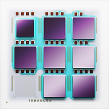
The POWER2, originally named RIOS2, is a processor designed by IBM that implemented the POWER instruction set architecture. The POWER2 was the successor of the POWER1, debuting in September 1993 within IBM's RS/6000 systems. When introduced, the POWER2 was the fastest microprocessor, surpassing the Alpha 21064. When the Alpha 21064A was introduced in 1993, the POWER2 lost the lead and became second. IBM claimed that the performance for a 62.5 MHz POWER2 was 73.3 SPECint92 and 134.6 SPECfp92.
The open source GCC compiler removed support for POWER1 (RIOS) and POWER2 (RIOS2) in the 4.5 release.
Description

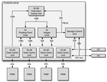
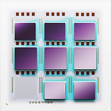
Improvements over the POWER1 included enhancements to the POWER instruction set architecture (consisting of new user and system instructions and other system-related features), higher clock rates (55 to 71.5 MHz), an extra fixed point unit and floating point unit, a larger 32 KB instruction cache, and a larger 128 or 256 KB data cache. The POWER2 was a multi-chip design consisting of six or eight semi-custom integrated circuits, depending on the amount of data cache (the 256 KB configuration required eight chips). The partitioning of the design was identical to that of the POWER1: an instruction cache unit chip, a fixed-point unit chip, a floating-point unit chip, a storage control unit chip, and two or four data cache unit chips.
The eight-chip configuration contains a total of 23 million transistors and a total die area of 1,215 mm. The chips are manufactured by IBM in its 0.72 μm CMOS process, which features a 0.45 μm effective channel length; and one layer of polysilicon and four layers of metal interconnect. The chips are packaged in a ceramic multi-chip module (MCM) that measures 64 mm by 64 mm.
POWER2+

An improved version of the POWER2 optimized for transaction processing was introduced in May 1994 as the POWER2+. Transaction processing workloads benefited from the addition of a L2 cache with capacities of 512 KB, 1 MB and 2 MB. This cache was implemented off-package with industry-standard burst SRAMs. The cache was connected to the POWER2+ via a 64- (for low-end systems) or 128-bit bus (for high-end systems). The cache was direct-mapped, had a 128-byte line size, and was write-through. The cache tags were contained on the storage control unit chip. The POWER2+ has a narrower 64- or 128-bit memory bus and a smaller 64 or 128 KB data cache. As there is less cache, the data cache unit chips are smaller as a result, and the revised storage control unit chip is also smaller. A goal for the six-chip configuration was to reduce cost, and therefore the chips are packaged in a solder ball connect (SBC) package instead of a MCM.
POWER2 Super Chip (P2SC)

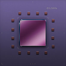
POWER2 Super Chip (P2SC) was released in October 1996 as the successor of the POWER2. It was a single-chip implementation of the eight-chip POWER2, integrating 15 million transistors on a 335 mm die manufactured in IBM's 0.29 μm five-layer metal CMOS-6S process. The first version ran at 120 or 135 MHz, nearly twice as fast as the POWER2 at 71.5 MHz, with the memory and I/O buses running at half speed to support the higher clock frequency. IBM claimed that the performance of this version was 5.5 SPECint95_base and 14.5 SPECfp95_base. A faster 160 MHz part fabricated in the 0.25 μm CMOS-6S2 process was announced at the Microprocessor Forum in October 1997.
The P2SC was not a complete copy of the POWER2, the L1 data cache and data translation lookaside buffer (TLB) capacities were halved to 128 KB and 256 entries, respectively, and a rarely used feature that locked entries in the TLB was not implemented in order to fit the original design onto a single die.
The P2SC was succeeded by the POWER3 as IBM's flagship microprocessor on the RS/6000 line in 1998. A notable use of the P2SC was the 30-node IBM Deep Blue supercomputer that beat world champion Garry Kasparov at chess in 1997. However, the computer's chess-playing capabilities were a result of its expert system running on custom VLSI chips, rather than the P2SCs.
See also
Notes
- "GCC 4.5 Release Series — Changes, New Features, and Fixes - GNU Project - Free Software Foundation (FSF)". gcc.gnu.org.
- Gwennap 1996
- White 1994
- Smith, Norris Parker (11 October 1996). "IBM LAUNCHES BRAND NEW CHIP FAMILY FOR THE RS/6000 LINE". hocwire.com. Retrieved 21 December 2021.
References
- Barreh, J. I.; Golla, R. T.; Arimilli, L. B.; Jordan, P. J. (September 1994). "POWER2 instruction cache unit". IBM Journal of Research and Development. 38 (5): 537–544. doi:10.1147/rd.385.0537.
- Ball, Richard (15 October 1997). "Chipville USA". Electronics Weekly.
- DeTar, Jim (22 August 1994). "IBM details Power2+; DEC bares new Alpha AXP". Electronic News.
- Gwennap, Linley (4 October 1993). "IBM Regains Performance Lead with Power2". Microprocessor Report.
- Gwennap, Linley (26 August 1996). "IBM Crams POWER2 onto Single Chip". Microprocessor Report.
- Hicks, T. N.; Fry, R. E.; Harvey, P. E. (September 1994). "POWER2 floating-point unit: Architecture and implementation". IBM Journal of Research and Development. 38 (5): 525–536. doi:10.1147/rd.385.0525.
- Lineback, J. Robert (28 June 1993). "IBM readies RISC Progeny in Unix". Electronic News.
- Shippy, David (9 August 1994). "The Power2+ Processor". Hot Chips 6.
- Shippy, D. J.; Griffith, T. W. (September 1994). "POWER2 fixed-point, data cache, and storage control units". IBM Journal of Research and Development. 38 (5): 503–524. doi:10.1147/rd.385.0503.
- Statt, Paul (January 1994). "Power2 Takes the Lead--For Now". Byte.
- White, S. W.; Dhawan, S. (September 1994). "POWER2: Next generation of the RISC System/6000 family". IBM Journal of Research and Development. 38 (5): 493–502. doi:10.1147/rd.385.0493.
Further reading
- Weiss, Shlomo; Smith, James Edward (1994). POWER and PowerPC. Morgan Kaufmann. ISBN 1558602798. — Chapter 6 describes the POWER2 architecture and processor